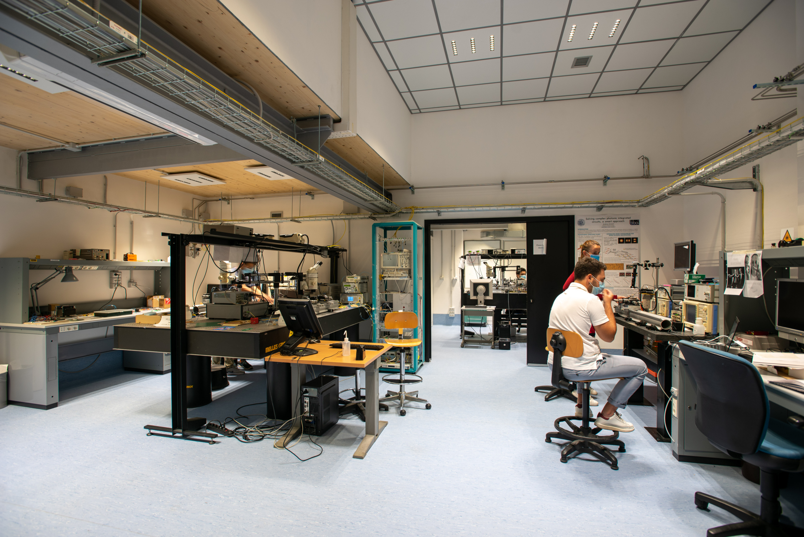
The laboratories of the Photonic Devices Group are equipped with five optical benches suitable for a broad range of measurement. Each setup is equipped with microscope and/or visible cameras; micro- and nano-positioning system for fibre and objective butt-coupling; thermo-electric controller for temperature stabilization of the samples; manual or automated polarization controllers; PC for bench management. Four setup are equipped with PC-controlled fibre positioning system and tapered/lensed fibres suitable for characterization of nano-waveguides. One setup is devoted to medium and large core waveguides or fibre characterization. Vertical mounting for grating coupler alignment are available and can be placed on any setup on request.
Waveguides and Devices Characterization
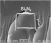
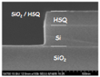
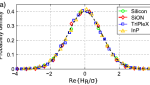
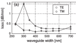
Tunable laser sources are available at wavelength 1.3 and 1.5 μm alongside with broadband sources, 980-nm sources for Erbium-doped fibre optical pumping and several EDFA amplifiers up to 1W output power. Five Optical Spectrum Analyzers (600nm-1700nm), an Optical Vector Analyzer, power meters, polarization meters, wavelength meters, visible and IR cameras complete the basic instrument set. The characterization of almost every optical parameter is available: spectral resolved attenuation and insertion loss, coupling efficiency, effective index, group index and chromatic dispersion, birefringence and space resolved birefringence, near field and refractive index reconstruction, back-scattering and polarization conversion, PDL and PMD. These characterization techniques have been tested on Ge:SiO2, SiON, Si3N4, TeO2, LiNbO3, InP, Chalcogenide, Silicon (SOI), Photonic Chrystal and Multimode waveguides. In the nonlinear domain typical characterizations include nonlinear absorption (TPA/FCA), spectral broadening, XPM and four wave mixing. In the wavelength range 1.52-1.56 μm a 27 dBm of average power is available (CW) with a maximum of 30W of pulse peak power with a repetition rate of 1 KHz.


Time Domain Characterization
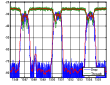
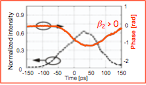
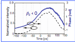
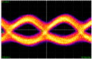
Transmission modules, a PRBS signal generator and phase/intensity modulators allows the generation of different signals up to 10 Gbit/s. A sampling oscilloscope, clock recovery and an integrated test board provide the capabilities for full time domain characterization of integrated optical devices. OOK, DPSK, DQPSK and polarization multiplexed signals can be generated and detected. EDFA amplifiers, fast detectors and more than 200 km of standard optical fiber (SMF 28) permit accurate and realistic transmission experiments. In addition, a unique virtual probe pulse technique is available for devices characterization in time domain. The envelope and the phase, that is the chirp, of single pulses propagating through devices can be accurately analyzed. Pulses from 1 ps to 500 ps offers the most accurate characterization conditions. The technique has been used to detect superluminal effects in integrated optical ring resonators.
Read more on:
M. Mattarei, A.Canciamilla, S. Grillanda, F. Morichetti, “Variable Symbol-Rate DPSK Receiver Based on Silicon Photonics Coupled-Resonator Delay Line,” Lightwave Technology, Journal of , vol.32, no.19, 2014 F. Morichetti, A. Melloni, and M. Martinelli, “Optical Pulse Coherence Interferometry: shaping probe pulses in time domain interferometry”, Optics Letters, vol. 15, no. 10, 1123-1125, May 2008. A. Melloni, F. Morichetti, “Direct Observation of Subluminal and Superluminal Velocity Swinging in Coupled Mode Optical Propagation”, Phys. Rev. Lett. 98, 173902 (2007)
Frequency Domain Reflectometry
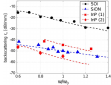
A powerful processing of the signal back-reflected from waveguides and devices allows to measure both amplitude and phase of distributed backscatter and localized reflections with a spatial resolution of tenths of micrometers. We used this technique to measure quantitatively the distributed backscatter of integrated optical waveguides in different technologies, including Photonic Crystals waveguides. Results concerning SOI and InP waveguides have been published on Physical Review Letters, Optics Letters, Applied Physics Letters and Advances in Optics and Photonics. The same characterizations have been performed on Ge:SiO2, SiON, Triplex and As2S3 waveguides. Polarimetric spatial topography of complex devices with a resolution of few tenth of micrometer is also possible.
Read more on:
D. Melati, A. Melloni and F. Morichetti, “Real photonic waveguides: guiding light through imperfections,” Adv. Opt. Photon. 6, 156-224 (2014) F. Morichetti, A. Canciamilla, M. Martinelli, A. Samarelli, R. M. De La Rue, M. Sorel, and A. Melloni, “Coherent backscattering in optical microring resonators,” Appl. Phys. Lett. 96, 081112 (2010). F. Morichetti, A. Canciamilla, C. Ferrari, M. Torregiani, A. Melloni, and M. Martinelli, “Roughness Induced Backscattering in Optical Silicon Waveguides,” Phys. Rev. Lett. 104, 033902 (2010). F. Morichetti, A. Canciamilla, and A. Melloni, “Statistics of backscattering in optical waveguides,” Opt. Lett. 35, 1777-1779 (2010).
Automatic Test Bench
A semi-automatic test bench for serial and repetitive measurements is available within the laboratories. The alignment is performed through two 6-axes nano-positioning stage for either standard or tapered fibres. The samples is hold by a vacuum – stabilezed chunk placed on a moving slide and the entire system can be fully controlled via a dedicated PC. A moving visible camera allow easy control of the operations directly on the computer monitor. The setup can be programmed to perform a sequence of measurements on different devices, comprising the fine alignment optimization essential for nano-waveguides. This test bench allows the full automation of all the characterization capabilities described in the previous sections, providing a fundamental tool for statistical investigations, wafer qualification, test pattern analyses and in general to speed up a large number of repetitive complex measurements.
……………………………………………………………………………………………………………………………………………..
![]()
Download the leaflet with lab description


