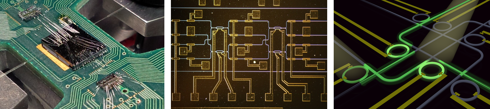
High complexity photonic integrated circuits
There is an ever increasing demand for complex photonic integrated circuits (PICs) able to perform advanced functions, like routing, (de)multiplexing and switching of optical signals, without any conversion in the electrical domain. Monitoring and control of complex PICs is now a hot topic in integrated photonics. Our research activity in this field aims to increase the ability to control complex PICs by means of new algorithms and strategies.
We offer opportunities of Master Degree theses focusing on some of the following tasks:
- (software) development of a software interface between a circuit-level photonic simulator (ASPIC) and Simulink/Matlab to test new control algorithm for PICs (in collaboration with the Israel Institute of Technology);
- (photonic circuits and testing) optical characterization and system-level testing of complex PICs, and implementation of the necessary control and calibration techniques to perform advanced functions;
- (electronic circuits and testing) test and development of a “plug & play” electronic board for the read-out of non-invasive integrated light detectors (CLIPPs) and for the feedback control of optical actuators integrated on a photonic chip (in cooperation with PoliMi’s electronic devices group, Prof. M. Sampietro);
- (optical coupling and characterization) development and characterization of new fiber-to-waveguide coupling techniques enabling the simultaneous coupling of up to 16 optical ports.
These activities will be carried out in the framework of the FP7 European project BBOI (www.bboi.eu)
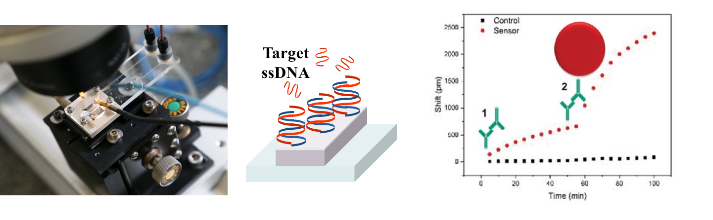
Biosensors through photonic integrated circuits
Optical communication is not the only field where photonic integrated circuits (PICs) contribute with improvements. Beside this field, sensors, and in particular biosensors, have become one of the emerging activities of our group, allowing to explore a multi-disciplinary path that includes concepts of chemistry, biology, electronics, and physics. The results will be a sensor capable of analysis biological solution and convert biological events into signals toward the use of PICs.
In this context, we offer opportunities of Master Degree thesis focusing on some of the following tasks:
- We propose a thesis that concerning the packaging of optical biosensor, in particular focusing on the functionalization of the PIC (how to place in a better way the receptors over the waveguide) and the microfluidic of the platform (how to carry biological solution over the sensing area). Activities: COMSOL modeling, fabrication, and testing;
- In collaboration with the group of prof. Bertacco, we propose a thesis based on a novel interaction between PICs and magnetic fields toward the use of magnetic nano-labels placed at the end of DNA sequences. Activities: COMSOL modeling and photonics testing;
- Based on a novel work we are conducting in collaboration with STm, we propose a thesis concerning the implementation and testing of a novel platform capable of tracking signals related to the smallest biological events occurring on the top of optical waveguides. Activities: Simulink modeling, photonics and electronics testing.
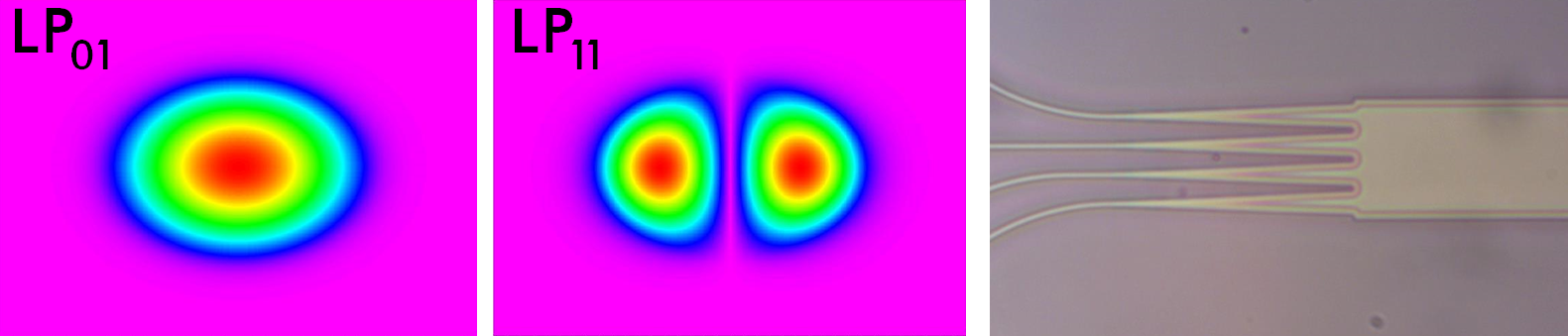
Photonic integrated circuits for high capacity optical links
Optical communications are evolving towards new transmission paradigms, where space division multiplexing (SDM) is being exploited in combination with conventional wavelength-division multiplexing (WDM) approaches to improve the capacity of optical fiber link. New generation photonic integrated circuits (PICs) able to manage aggregated SDM-MDM channels are required.
In this context, we offer opportunities of Master Degree thesis focusing on some of the following tasks:
- (optical coupling and characterization) development and characterization of new fiber-to-waveguide coupling techniques enabling the coupling few mode fibers (FMF) with multimode waveguide structures;
- (photonic devices and testing) optical characterization and system-level testing of MDM-WDM transmitters and receivers realized in Indium Phosphide and /or Silicon Photonics technologies;
These activities will be carried out in the framework of the FP7 European project BBOI (www.bboi.eu)
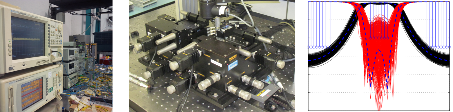
Automated testing of photonic integrated circuits
Standardization of photonic integrated circuits (PICs) is a key step for a massive diffusion of photonic technologies. This process requires the possibility to automatically test hundreds of PICs, providing a statistical database to perform tolerance analyses, yield estimation procedures, and indentify robust design-on-tolerance approaches. The Photonic Devices Lab has been recently equipped with a PC-assisted semi-automatic optical test bench that is suitable for systematic characterization of PICs.
In this context, we offer opportunities of Master Degree thesis focusing on some of the following tasks:
– (equipment and software) hardware and software (LABVIEW) setup and calibration of the semi-automatic optical test bench. Free courses of LABVIEW will be offered to students during the thesis.
– (statistical analysis) development of statistical analysis techniques and generation of realistic (statistical) models of photonic integrated devices. This activity will be carried out in collaboration with world-renowned European photonic foundries;
– (optical design) design and optimization of photonic integrated structures for automated systematic characterization and wafer level testing procedures
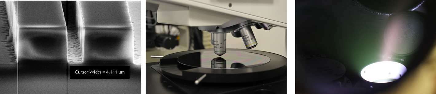
Photonics technologies and material characterization
The Photonic Devices Lab operates next-door with the new-born clean room of PoliFab (http://www.polifab.polimi.it/), the micro- and nanofabrication centre of Politecnico di Milano.
We offer opportunities of Master Degree thesis focusing on the deposition and characterization of Silicon Oxynitride (SiON), Silicon Oxycarbide (SiOC), amorphous Silicon (a-Si) films for integrated photonics applications. Candidates will have the opportunity to learn how to perform lithography, etching, and many other steps necessary for the realization of an intergrated photonic circuit.
Interests in physics and chemistry are recommended.
Developing of a circuital simulator for integrated photonics
The Photonic Devices Group has developed in the years the first circuital simulator for integrated photincs. We are looking for students motivated to work in an international context (European projects) for the developing of the Aspic simulator (www.aspicdesign.com).
The actvities for a Master Degree thesis are:
- development of the graphic user interface;
- numeric techniques for the design and analysis of complex circuits;
- design of integrated photonic circuits by means of the “generic foundry” paradigm;
- software implementation of CAD tools.
The activities will be carried out at the PoliFab laboratories (Via Giuseppe Colombo 81).