 For an optical designer, waveguides play the same role as paintbrushes do for a painter. Always use the one that better fits your project.
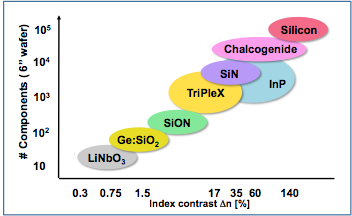
And the first choice to be done is the refractive index contrast of the waveguide, this parameter setting the main characteristics of light propagation and the scale of integration of photonic devices. This choice is often a bit tricky, because every optical technology is a world apart, with its own rules, advantages and limitations.
This is the reason why at Politecnico di Milano we have invested many years of our research activity to gain experience in variety of different optical platforms:
as a result now we have state-of-the-art design and characterization techniques for most of the technologies of interest in photonics, from very low index contrast glass waveguides (that too often are improperly considered the “past” of integrated optics) to the new frontier of very high index contrast optical waveguides.
Read more on:
A. Melloni, R. Costa, G. Cusmai, F. Morichetti , “The role of index contrast in dielectric optical waveguides,” International Journal of Materials and Product Technology, vol. 34, no. 4 pp. 421 – 437, Apr. 2009Silicon Photonics: the future is here
 Silicon photonic technology allows a very high components miniaturization, reaching a complexity of thousands of components in a footprint of less than 1 mm2. It can provide low-loss waveguides and germanium can be integrated for light detection purposes for detection purposes in the 1500-1600 nm wavelength range although silicon waveguides can be used efficiently even in the near and mid infrared range. Silicon allows for very fast reconfiguration capabilities to obtain, by means of integrated actuators, low-power high speed optical modulators, efficient “slow” thermal reconfiguration. Many efforts have been put in the last years to develop silicon photonics technologies that are “CMOS-compatible”, meaning that their implementation does not require any alteration of the standard fabrication process employed for CMOS electronics. With CMOS-compatible silicon photonics technologies it is also possible to integrate monolithically on the same chip the electronics and photonics, allowing to directly manage each photonic device (in terms of delivery of the electric signals for tuning, feedback, bias) enabling complex optoelectronic circuits while potentially reducing the cost of the system.
Read more on:
A. Melloni, A. Annoni, S. Grillanda, D. Melati and F. Morichetti, “Control, configuration and stabilization of photonic integrated circuits,” 2016 21st OptoElectronics and Communications Conference (OECC) held jointly with 2016 International Conference on Photonics in Switching (PS), Niigata, Japan, 2016, pp. 1-3. (invited paper)Indium Phosphide, one semiconductor to rule them all
 Indium Phosphide is a binary semiconductor that emerged as one of the most promising and versatile technology for the integration of numerous different functionalities. The opportunity to grow active materials alongside passive layer stacks in a feasible and reproducible manner, enabled monolithic integration of complex circuits comprising sources, amplifiers and detectors together with passive circuitry as power splitters, waveguides or filters. Indium Phosphide-based photonic circuits offered innovative solutions for telecommunication applications, as wavelength division multiplexing routers and transceivers or complex switching structures. Even microwave photonics and THz signal generation are among the fields where these devices can be competitive.
Read more on:
Meint Smit et al., “An introduction to InP-based generic integration technology”, 2014 Semicond. Sci. Technol. 29 083001;Tailoring the refractive index contrast… Yes, we can! (TriPleX technology)
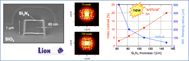
Is it possible to tailor the refractive index contrast arbitrarily over a continuous range?
Now it is, with TriPleX technology (http://www.lionixbv.nl/integratedoptics/triplex.html). Simply arranging a few layers of two conventional materials a box-shaped waveguide can be realized, consisting of a thin high index coating layer (silicon nitride) encapsulating a low-index inner material (silica). Only acting on the waveguide geometry and without changing the refractive index of the materials, which are conveniently kept to stoichiometric composition, different confinement regimes can be achieved and optimized to the specific application. Waveguide birefringence and polarization dependent loss can be adjusted at a will by slightly changing the waveguide geometry.
Propagation losses as low as the state-of-the-art low-index-contrast waveguides (< 0.1 dB/cm), very low PDL (< 0.1 dB/cm), and easy interconnection with optical fibers (< 0.15 dB/facet) have been demonstrated in single mode box-shaped waveguides.
Read more on:
F. Morichetti, A. Melloni, M. Martinelli, R.G. Heideman, A. Leinse, D.H. Geuzebroek, and A. Borreman, “Box-shaped dielectric waveguides: a new concept in integrated optics?,” Journal of Lightwave Technology, vol. 25, no. 9, pp. 2579-2589, Sept. 2007. (invited paper)Get rid of imperfections: light up chalcogenide waveguides
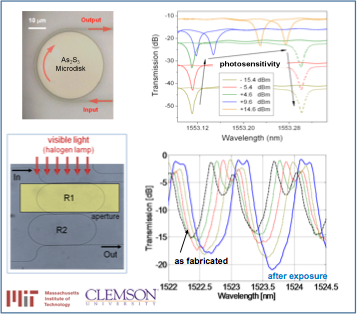 One of the main limits of large-scale-of-integration photonics is the strong sensitivity to fabrication tolerances. A deviation of 1 nm in the width of a high-index-contrast waveguide causes as much as 1 nm wavelength shift of the spectral response of any interferometric device. This makes devices with a bandwidth of a few tens of GHz hardly realizable even with an atomic scale control of the waveguide writing process.
Post-fabrication treatments that permanently compensate for fabrication imperfections are thus required to locally “repair” integrated devices and to reach desired specifications with no need for a continuous active tuning.
The intrinsic photo-sensitivity of chalcogenide glass materials can be utilized to this aim. Visible light trimming has been exploited to fine-tune the effective refractive index of As2S3 waveguides, and thereby the resonant wavelength of micro-ring and micro-disk resonators. With this approach the performance of coupled resonator filters with up to four ring resonators in As2S3 glass technology was optimized. A trimming velocity as high as 0.25 nm/minute was achieved with a light intensity of only 2 mW/cm2, and no significant relaxation effects have been observed within a time scale of several weeks since the light exposure.
Read more on:
N. Carlie, J. D. Musgraves, B. Zdyrko, J. Hu, A. Canciamilla, F. Morichetti, V. Singh, A. Agarwal, I. Luzinov, K. Richardson, L. C. Kimerling, and A. Melloni, “Integrated chalcogenide waveguide resonators for mid-IR sensing: Leveraging material properties to meet fabrication challenges,” Opt. Express, vol. 18, no. 25, pp. 26728-26743, Dec. 2010 (invited paper).as a result now we have state-of-the-art design and characterization techniques for most of the technologies of interest in photonics, from very low index contrast glass waveguides (that too often are improperly considered the “past” of integrated optics) to the new frontier of very high index contrast optical waveguides.
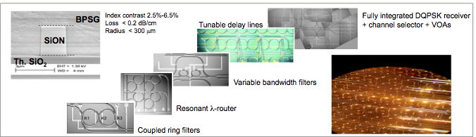
Medium index contrast glass (SiON): in medio stat virtus…
Silicon Oxynitride is one of the best and most exploited glass technologies for medium and high contrast integrated optics, namely in the range from 2% to more than 10%. It permits to realize waveguides with a very low propagation loss (0.2 dB/cm), low polarization sensitivity, efficient interconnection with optical fibers, bending radius down to 100μm or even less, and hence it enables to integrate many functions in a small footprint chip. The process is CMOS compatible and can be joined to other platforms (such as silicon on insulator) to realize advanced complex devices.
Read more on:
F. Morichetti, R. Costa, G. Cusmai, A. Cabas, M. Ferè, M.C. Ubaldi, A. Melloni, M. Martinelli, “Integrated optical receiver for RZ-DQPSK transmission systems”, Proc. Optical Fiber Communication Conference (OFC), paper FC8, Los Angeles 2004 F. Morichetti, A. Melloni, A. Breda, A. Canciamilla, C. Ferrari, and M. Martinelli, “A reconfigurable architecture for continuously variable optical slow-wave delay lines”, Optics Express, vol. 15, no. 25, pp. 17273-17282, Dec. 2007. A. Melloni, F. Morichetti, G. Cusmai, R. Costa, A. Breda, C. Canavesi, M. Martinelli, “Progress in large integration scale circuits in SiON technology”, Proceed. of the 9th International Conference on Transparent Optical Networks, Rome (Italy), vol. 1, pp. 223-226, 1-5 July 2007. F. Morichetti, A. Melloni, C. Ferrari and M. Martinelli, “Error-free continuously-tunable delay at 10 Gbit/s in a reconfigurable on-chip delay-line,” Optics Express, vol. 16, no. 10, pp. 8395-8405, May 2008.Low index contrast glass (Ge:SiO2): classic is always fashionable
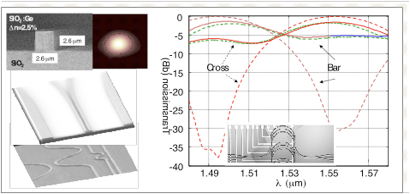 In an era where photonics is every day pushing a little bit forward the scale of integration, low index contrast glass technologies still offer the most established solutions to integrate a limited number of functions on a single optical chip, guaranteeing device reliability, fast time to market and relatively low cost.
Germanium doped silica (Ge:SiO2) waveguide now reliably cover an index contrast range from less than 1% to up to 2.5 %, enabling the realization of quite complex photonic architectures, including multi-path Mach-Zehnder interferometers, lattice filters, wavelength selectors, gain flattening filters, chromatic dispersion compensator and array waveguide grating. Loss performance, polarization sensitivity, tolerance to fabrication imperfection, thermal stability, and ultimately yield is still superior to any other photonic platform.
Pingback: Optical Waveguides | Photonic Devices Group