In 2014 we have conceived and developed CLIPP (Contactless Integrated Photonic Probe), that is the first integrated device enabling noninvasive light observation in optical waveguides.
CLIPP: The first integrated light observer
The CLIPP concept
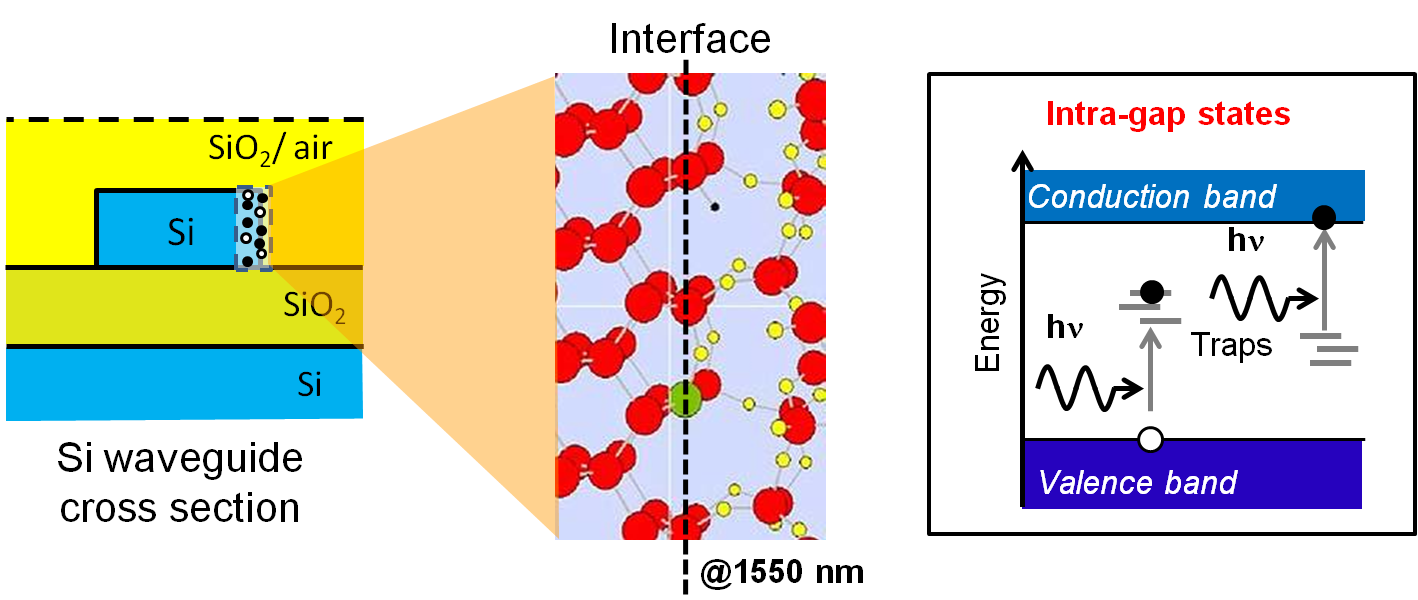 Near-infrared light propagating in semiconductor waveguides (such silicon or indium posphide) leaves some footprints behind. Despite material transparency, free carriers are generated at the core/cladding interface due to surface state absorption (SSA), occurring in the first 2-3 silicon atomic layers.
CLIPP is able to detect these carriers and infer information on how many photons have passed through the waveguide.
And this can be done without wasting any extra photon.
How to do it (in a lab)…
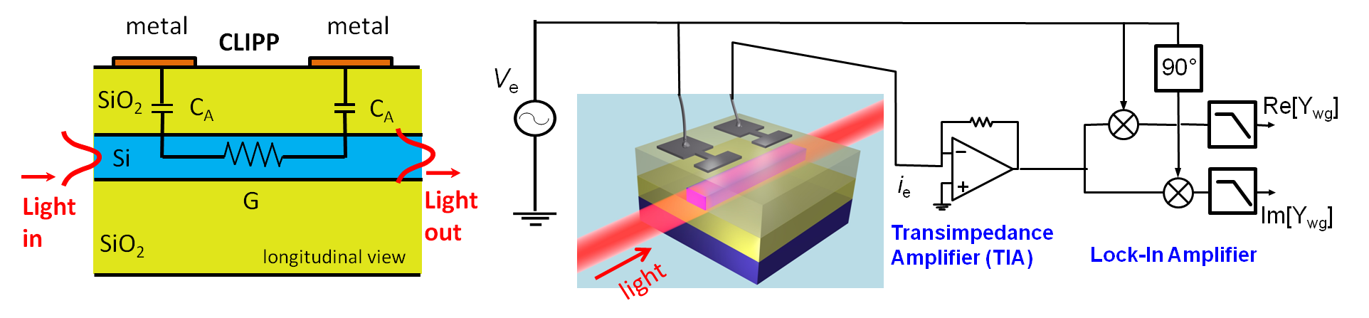
To be truly noninvasive, the waveguide must remain completely untouched. To this aim, CLIPP performs a “remote” sensing: the light-dependent change of the electrical conductivity of the waveguide is measured though a contactless capacitive access to the waveguide core. All we need is a two-electrode arrangement, driven at a suitable a.c. voltage, and a high sensitivity impedance measurement system based on a low noise transimpedance amplifier and a lock-in detector.
…. how to do it (everywhere) 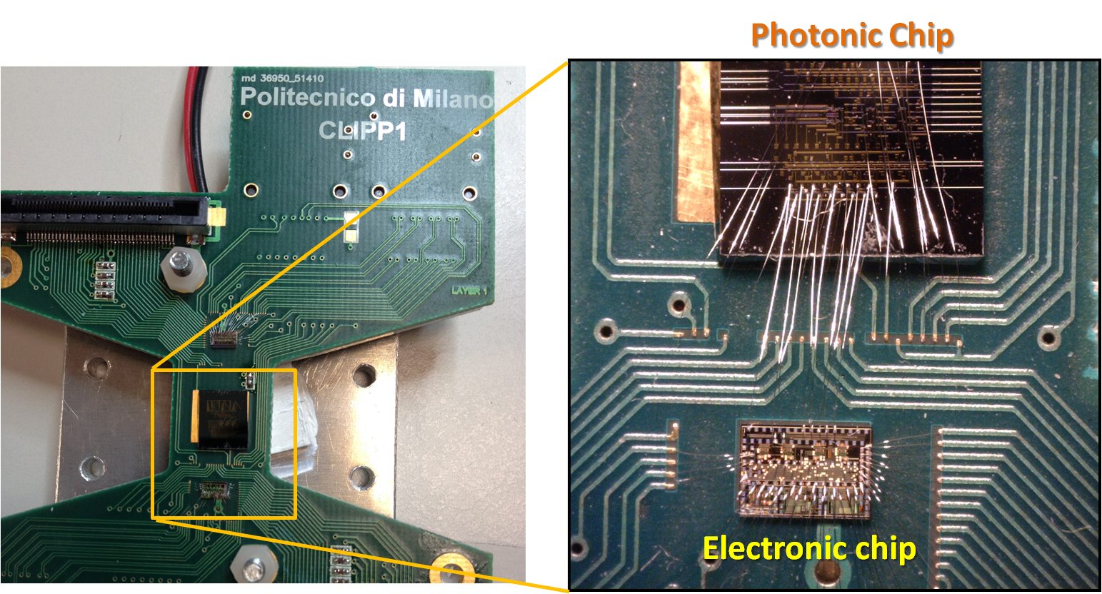
High sensitivity does not mean complexity.
The CLIPP read-out system can be integrated on a CMOS ASIC bridged to the silicon photonic chip and mounted on the same printed circuit board. The use of standard CMOS electronics makes the CLIPP concept directly exploitable in system-level applications. The compactness and scalability of CMOS electronics to multichannel read-out systems allows to extend this approach to to monitorign and feedback control of complex integrated circuits hosting many photonic components
CLIPP performance: high sensitivity, no light perturbation
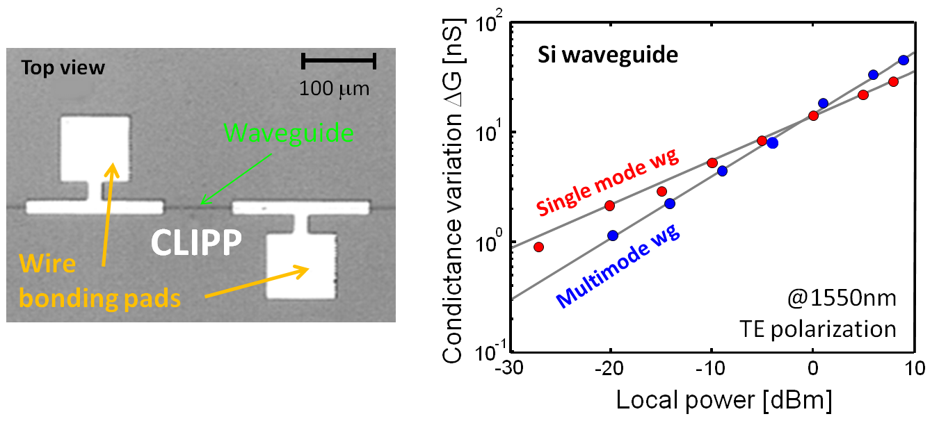 The CLIPP concept has been demonstrated in silicon and indium phosphide technologies. The CLIPP can be very compact (less than 100 μm length), work on single-mode and multi-mode waveguides, and on both polarizations (TE/TM). Light intensity monitoring can be performed with a sensitivity down to -30 dBm, 40 dB dynamic range and μs-scale time response.
The CLIPP is a truly transparent in-line light detector. It introduces neither loss nor amplitude modulation. An extremely small phase modulation was observed (<1 mrad), corresponding to < 0.5 ppm perturbation of the waveguide effective index (comparable to 3 mK fluctuations). This perturbation is negligible even for resonators with a Q factor of up to 1,000,000.
CLIPP applications:
Multipoint monitoring of PICs.
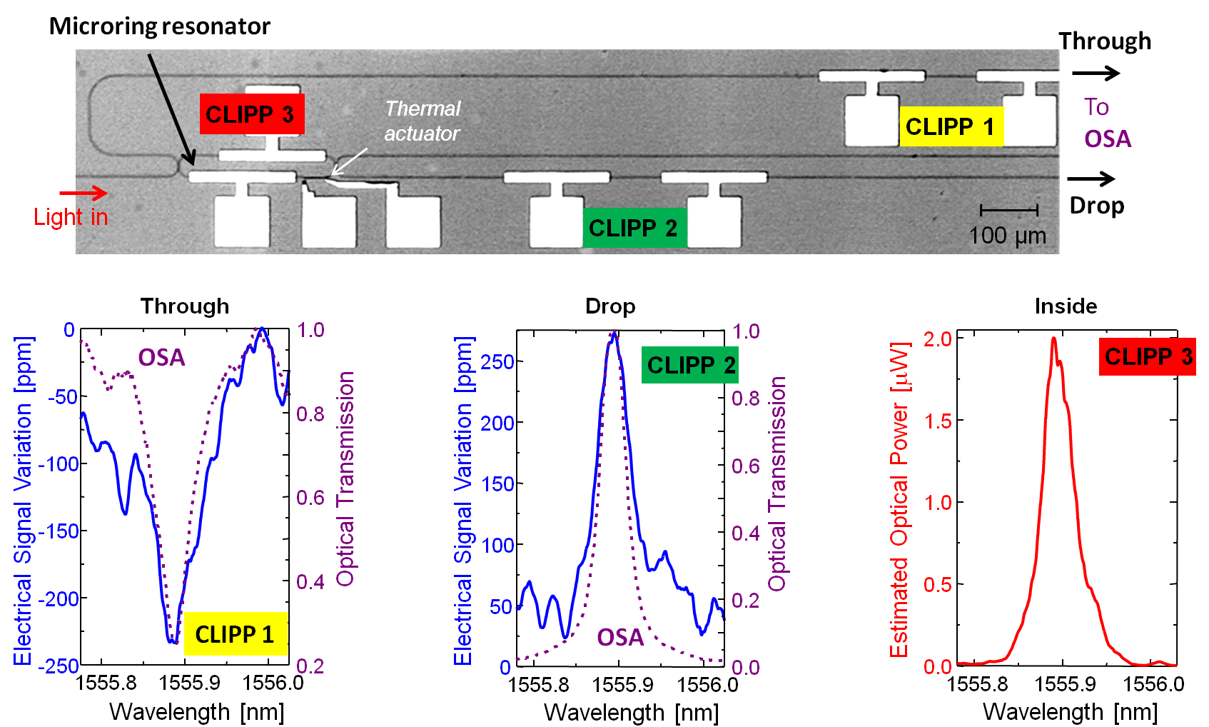
Compactness, light transparency, ease of fabrication and simultaneous read-out of many channels trough CMOS electronics enable the integration of many CLIPPs inside generic PICs without constraining the design and technology of the waveguide underneath. Many light monitors can be placed in strategic positions around the chip enabling real time management of complex integrated optical systems. For instance, we fabricated silicon microring resonators with CLIPPs integrated at the Through and Drop ports, and inside the resonator itself, thus accessing information not available with conventional photodetectors.
Automated tuning, feedback locking and stabilization.
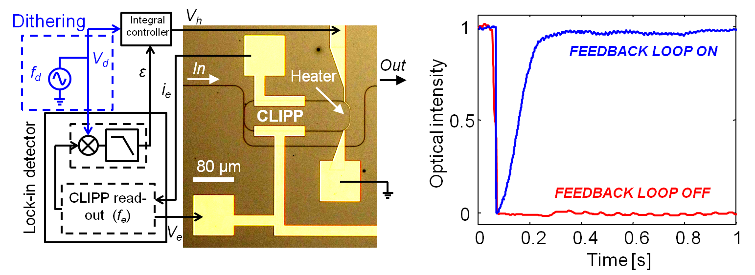 The CLIPP can be used as a transparent detector for the realization of local feedback loops, thus making the control of devices integrated into complex circuits as if they were stand-alone. For instance, we have integrated a CLIPP inside thermally actuated microring resonator and exploited is as a monitor to automatically tune the ring’s resonance to overlap with the wavelength of an external laser. After tuning, in order to have the resonator wavelength always locked to that of the laser, the CLIPP continuously monitors the intracavity optical intensity, providing a feedback error signal to the thermal actuator steering the resonance of the ring.
Automated fiber to waveguide alignment.
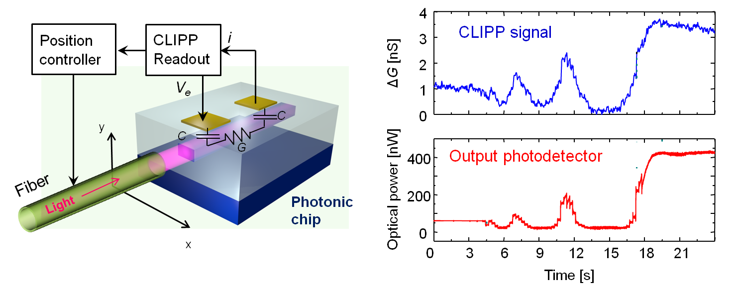 The CLIPP can be effectively used to assist fiber-to-waveguide alignment procedures. Coupling efficiency is monitored trough a CLIPP realized near the chip input facet that provides a feedback electrical signal steering the fiber positioning system. Automated single fiber to silicon nanowaveguide coupling was demonstrated with 40 nm resolution in a time scale of a few seconds. This approach holds for both butt-coupling and vertical coupling, makes the fiber alignment procedure independent of the optical circuit integrated on the photonic chip, removes the need for simultaneous alignment of an output fiber, and thus eases optical chip characterization, wafer-level testing, and packaging of photonic devices
Spotlights on CLIPP
“Silicon photonics: Stalking light“, Nature Photonics 8, 2014
“Controlling Photonic Circuits, Noninvasively,” Optics and Photonics News, September 2014
CLIPP on the news
Press gallery: ANSA, Le Scienze, Galileo.it, Ingegneri.info, Italian network (italian)
“Mesurer la lumière sans absorber de photons”, bulletins-electoniques.com (french)
Press release by the Politecnico di Milano (italian)
Interview with Francesco Morichetti, Il Sussidiario.net (italian)
Read more on CLIPP
1. F. Morichetti, S. Grillanda, M. Carminati, G. Ferrari, M. Sampietro, M. J. Strain, M. Sorel, and A. Melloni, “Non-invasive on-chip light observation by contactless waveguide conductivity monitoring,” J. Selected Topics in Quantum Electronics, vol. 20, no. 4, Jul./Aug. 2014.
2. S. Grillanda, M. Carminati, F. Morichetti, P. Ciccarella, A. Annoni, G. Ferrari, M. Strain, M. Sorel, M. Sampietro, A. Melloni, “Noninvasive monitoring and control in silicon photonics using CMOS integrated electronics,” Optica, vol.1 no. 3, pp. 129-136, Sep. 2014.
3. M. Carminati, S. Grillanda, P. Ciccarella, G. Ferrari, M. J. Strain, M. Sampietro, A. Melloni, and F.Morichetti, “Fiber to waveguide alignment assisted by a transparent integrated light monitor,” IEEE Photonic Technology Letters, vol. 25, no.5 , pp. 510-513, Dec. 2014.
4. S. Grillanda, F. Morichetti, N. Peserico, P. Ciccarella, A. Annoni, M. Carminati, and A. Melloni, “Non-Invasive monitoring of mode-division multiplexed channels on a silicon photonic chip,” J. Lightwave Technology, in press (10.1109/JLT.2014.2377558).
Related projects
The CLIPP research activity is being carried out within the framework of the EU Project BBOI.
Pingback: Non invasive light observation | Photonic Devices Group
Pingback: Morichetti’s invited talk at OFC 2016 | Photonic Devices Group