Open the door to foundries of the future

Over the last decades, integrated photonics has experienced a large widening of its application fields. Telecommunication, sensing, medical/biological applications, microwave filtering, long-wavelength devices can benefit of the advantages of photonic integration. On the other hand, it also emerged how a very small number of promising photonics devices resulted at the end in commercial products available on the market, enlightening the limits of the current production chain.
Together with many international partners, we are actively working to create and put in place all the instruments that will allow in the near future a complete paradigm shift in the production of photonic circuits.
Towards fabless approach for photonics
As a projects grow more and more in complexity and inventiveness, an intrinsic limit to the real widespread of integrated photonics appears in the methodology adopted for the development and fabrication of the circuits. What is urgently needed is the availability of stable and cost-effective technological processes that can be exploited by many users for the realization of photonic circuits. This idea relies on the development of few standard integration technologies not oriented to a single high performance application but rather able to offer the most used components optimizing their functionalities and guaranteeing their characteristics. If each single device exhibits a repeatable behaviour, their combination can likely results in circuits with higher complexity and better performances.
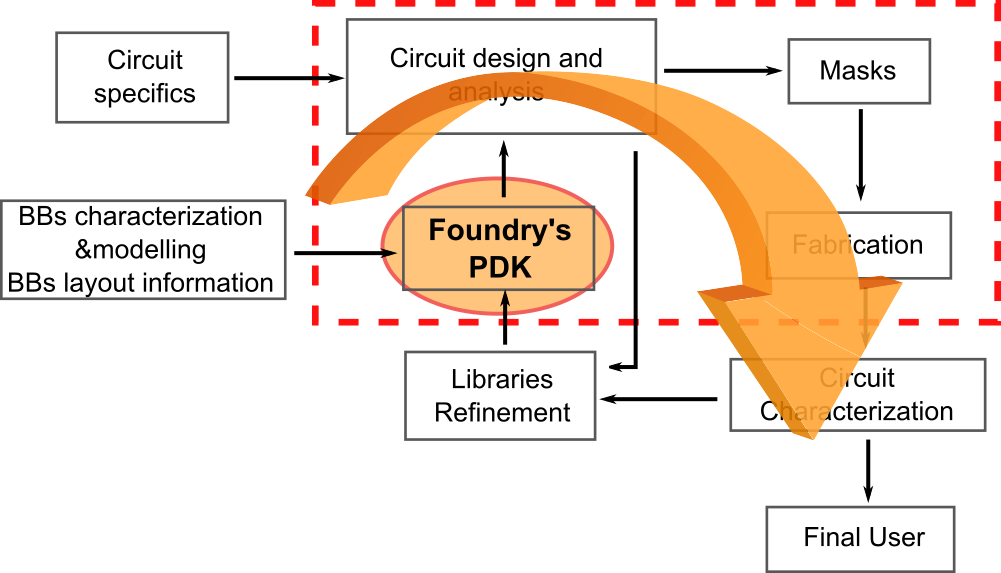
A generic foundry (as a foundry adopting this manufacturing approach is commonly named) that has reached the maturity and reliability level for a competitive entry into the market can be made available to a large number of external users with low entry cost. This can be realized through Multi Project Wafer runs (MPWs) that aggregate the design of many users into a single process run, fabricating all the chip together on the same wafers. The area available on any wfer is subdivided in unitary cell and each one sold to one of the users. This approach is clearly convenient for small groups and R&D projects which generally involve small sample volumes and could not sustain alone the effort of a fully dedicated run.
Design Kits for photonics
A key instrument is fundamental to allow the users an easy access this new approach: Process Design Kits (PDKs). PDKs must become the core interface instruments between foundries and users, an element that allows to standardize the circuits design flow making it more advanced and suited for very large circuits and hence to fully exploit the potentialities offered by MPWs. The creation of PDKs is then the keystone for the success of the reorganization of the PICs production.
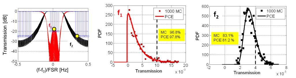
Inside a PDK a full library of BBs is made available to the user, each one bringing information related to layout, layer stack, design rules, physical properties and optical behaviour. This collection of information and data referring to a single component forms the Building Block. The description of its optical characteristics is of particular importance and the definition of proper synthetic models of the behaviour of each device permits to exploit simulations at circuital level instead relying every time on directly time-consuming electromagnetic simulations.
Building a valuable PDK
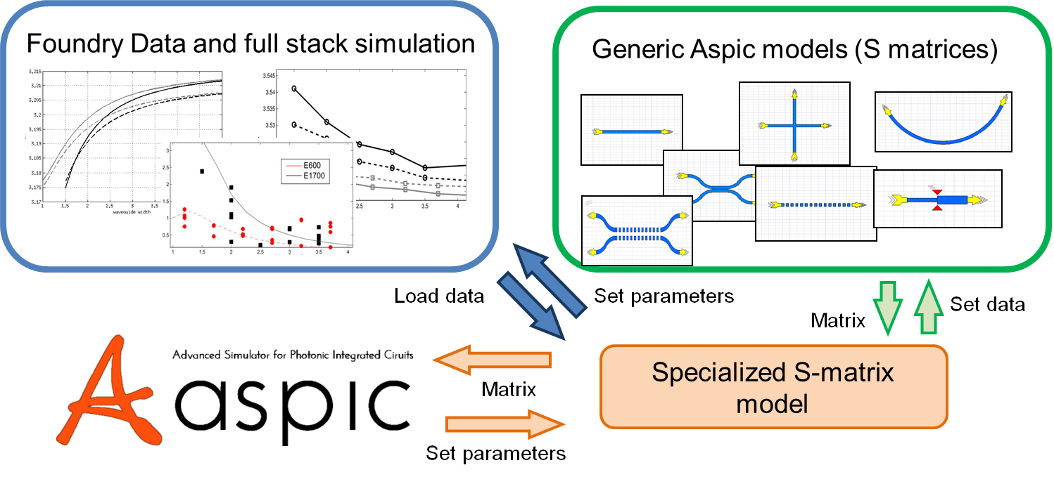
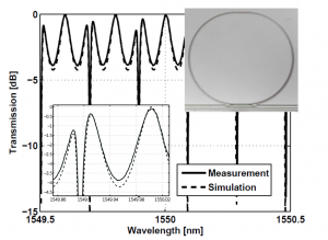
The translation between technological aspects and parameters to PDK is related to two aspects: the theoretical model and the experimental data. Modelling and characterizations cannot be separate if our goal is the creation of a PDK for a specific foundry. Pure theoretical models are empty objects, describing only virtual components not related to a real process. We could even say that characterizations themselves are what drive and guide the definition of the proper models in each case. The mathematical formulation has hence to be completed with process-specific data (optical properties, electrical behaviour, parameters statistics, yield information, etc.) which can be acquired only by the experimental characterization of each component. Realistic models including complex aspects of their behaviour require refined characterization techniques in order to permit the measurement of subtle aspects of the transfer function of a device and to include them in the BB structure.
Read more on PDKs
1. D. Melati, F. Morichetti, A. Canciamilla, D. Roncelli, F. M. Soares, A. Bakker, and A. Melloni, “Validation of the Building-Block-Based Approach for the Design of Photonic Integrated Circuits,” J. Lightwave Technol. 30, 3610-3616 (2012) http://www.opticsinfobase.org/jlt/abstract.cfm?URI=jlt-30-23-3610
2. Meint Smit et al., “An introduction to InP-based generic integration technology”, 2014 Semicond. Sci. Technol. 29 083001 doi:10.1088/0268-1242/29/8/083001
3. D. Melati, “A design kit perspective on InP-based photonic integrated circuits”. PhD Thesis, Italy (2014) http://hdl.handle.net/10589/89724
4. Jeppix web site
Related projects
The research activity on PDKs is mainly being carried out within the EU Project PARADIGM.